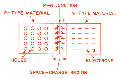
What is the formation of PN-Junction?
Category: Electronics Articles
14 Dec 14
- A P-type and N-type semiconductor are joint together with a help of special fabrication techniques to form a PN-Junction.
- The terminals are brought out for external connection with P-type and N-type semiconductor.
- The P side is called as anode and N side is called as cathode.
- The PN Junction forms a basic semiconductor device called diode.
- In a PN-junction, when the electrons and holes move to the other side of the junction, they leave behind exposed charges on dopant atom sites, which are fixed in the crystal lattice and are unable to move.
- The electric field Ê forms between the positive ions cores in the n-type material and negative ion cores in the p-type material.
- This electric field created by the diffusion process has created a “built-in potential difference” across the junction with an open-circuit (zero bias) potential of:
 Where: Eo is the zero bias junction voltage, VT the thermal voltage of 26mV at room temperature, ND and NA are the impurity concentrations and ni is the intrinsic concentration.


